BJT 프로세스 이해
목차
개요 BJT 프로세스
바이폴라 접합 트랜지스터(BJT) 공정은 반도체 전자 분야의 기본 개념입니다. BJT는 전류를 증폭하는 능력으로 인해 많은 전자 장치에 필수적인 구성 요소입니다. 이 가이드에서는 BJT 프로세스의 유형, 특성, 응용 분야, 장점 및 단점을 포함하여 BJT 프로세스에 대한 심층적인 탐색을 제공합니다. 또한 BJT 제조에 사용되는 특정 금속 분말 모델을 자세히 살펴보고, 정보에 입각한 결정을 내릴 수 있도록 철저한 비교를 제공합니다.
BJT의 종류와 특성
NPN 및 PNP BJT
BJT는 크게 두 가지 유형이 있습니다: NPN과 PNP입니다. 두 유형 모두 동일한 원리로 작동하지만 구성과 전하 캐리어 이동에 차이가 있습니다.
유형 | 구성 | 충전 통신사 | 기호 |
---|---|---|---|
NPN | 이미터(N) - 베이스(P) - 콜렉터(N) | 전자 | NPN 기호 |
PNP | 이미터(P) - 베이스(N) - 콜렉터(P) | 구멍 | PNP 기호 |
BJT 재료의 구성 및 특성
BJT에 사용되는 재료는 성능에 매우 중요합니다. 실리콘(Si)과 게르마늄(Ge)이 주로 사용되는 반도체입니다.
재료 구성 및 특성
재질 | 구성 | 속성 | 애플리케이션 |
---|---|---|---|
실리콘(Si) | 인(N형) 또는 붕소(P형)와 같은 도핑 원소가 포함된 순수 실리콘 | 높은 열 안정성, 낮은 누설 전류 | 범용 트랜지스터, 전력 장치 |
게르마늄(Ge) | 유사한 도핑 원소를 가진 순수 게르마늄 | 더 높은 전자 이동성, 더 낮은 열 안정성 | 고주파 애플리케이션, 저전압 디바이스 |
애플리케이션 기호
BJT는 다양한 애플리케이션에 사용되는 다용도 부품입니다. 아래는 몇 가지 주요 용도를 요약한 표입니다.
BJT의 애플리케이션 및 용도
애플리케이션 | 설명 | 예제 |
---|---|---|
증폭 | BJT는 전류를 증폭하므로 오디오 및 무선 주파수 장치에 필수적입니다. | 오디오 증폭기, RF 증폭기 |
전환 | 회로에서 전자 신호를 켜고 끄는 데 사용됩니다. | 디지털 회로, 마이크로프로세서 |
진동 | BJT는 진동 회로를 만드는 데 필수적인 요소입니다. | 신호 발생기, 오실로스코프 |
규정 | 일정한 전압 레벨을 유지하기 위해 전압 조정 회로에 사용됩니다. | 전원 공급 장치, 전압 조정기 |
사양, 크기, 등급 및 표준
BJT는 다양한 애플리케이션에 맞게 다양한 사양으로 제공됩니다. 이러한 사양을 이해하면 필요에 맞는 올바른 BJT를 선택하는 데 도움이 될 수 있습니다.
사양 및 표준
사양 | 설명 | 성적 예시 |
---|---|---|
전압 등급 | 트랜지스터가 처리할 수 있는 최대 전압입니다. | 30V, 60V, 100V |
전류 등급 | 트랜지스터가 전도할 수 있는 최대 전류. | 100mA, 1A, 10A |
전력 손실 | 트랜지스터가 손상 없이 발산할 수 있는 최대 전력. | 200mW, 500mW, 1W |
주파수 응답 | 트랜지스터가 효과적으로 작동할 수 있는 최대 주파수입니다. | 100MHz, 300MHz, 500MHz |
공급업체 및 가격 세부 정보
여러 공급업체에서 고품질 BJT를 제공합니다. 가격은 사양, 수량 및 공급업체에 따라 다릅니다.
BJT 공급업체 및 가격
공급업체 | 제품 | 가격 범위(단위당) |
---|---|---|
텍사스 인스트루먼트 | 범용 BJT | $0.10 – $1.00 |
온세미컨덕터 | 고주파 BJT | $0.20 – $2.00 |
페어차일드 반도체 | 전력 BJT | $0.50 – $3.00 |
NXP 반도체 | 저소음 BJT | $0.15 – $1.50 |
인피니언 테크놀로지스 | BJT 전환 | $0.25 – $2.50 |
BJT의 장단점 비교
BJT는 다양한 애플리케이션에 대한 적합성에 영향을 미치는 다양한 장점과 한계가 있습니다.
BJT의 장점과 한계
측면 | 장점 | 단점 |
---|---|---|
성능 | 높은 전류 이득, 빠른 스위칭 | FET에 비해 더 높은 전력 소비 |
비용 | 일반적으로 낮은 비용 | 고성능 모델의 경우 더 높은 비용 발생 가능성 |
열 안정성 | Si BJT의 열 안정성 향상 | Ge BJT의 열 안정성 저하 |
주파수 응답 | Ge BJT의 고주파 작동 | 기생 커패시턴스에 의해 제한됨 |
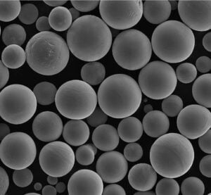
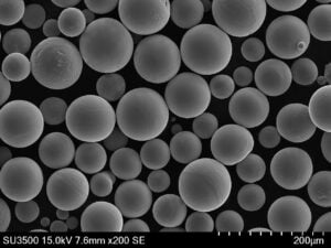
BJT 제조의 금속 분말 모델
BJT 제조 공정에는 다양한 금속 분말 모델이 사용됩니다. 이러한 재료는 최종 제품의 효율성과 성능에 영향을 미칩니다.
특정 금속 분말 모델
- 구리(Cu) 분말
- 설명: 전기 전도성 향상을 위해 사용되는 전도성이 높은 금속 분말.
- 애플리케이션: 전력 애플리케이션용 고성능 BJT에 사용됩니다.
- 속성: 뛰어난 열 및 전기 전도성.
- 알루미늄(Al) 분말
- 설명: 가볍고 전도성이 좋은 알루미늄 파우더는 특정 BJT 애플리케이션에 사용됩니다.
- 애플리케이션: 경량 및 높은 열 전도성 요구 사항을 위해 BJT에 사용됩니다.
- 속성: 우수한 전도성, 경량.
- 니켈(Ni) 분말
- 설명: 내식성과 안정성으로 유명합니다.
- 애플리케이션: 내구성이 중요한 환경에서 사용.
- 속성: 부식에 대한 높은 내성, 안정적인 성능.
- 철(Fe) 분말
- 설명: 가용성과 자성 특성으로 인해 일반적으로 사용됩니다.
- 애플리케이션: 자성 특성이 필요한 BJT에 사용됩니다.
- 속성: 마그네틱, 비용 효율적.
- 은(Ag) 분말
- 설명: 금속 중 가장 높은 전기 전도성을 제공합니다.
- 애플리케이션: 정밀 애플리케이션을 위한 하이엔드 BJT에 사용됩니다.
- 속성: 우수한 전기 전도성, 고가.
- 금(Au) 분말
- 설명: 전도성이 뛰어나고 산화에 강합니다.
- 애플리케이션: 중요하고 신뢰성이 높은 애플리케이션을 위한 BJT에 사용됩니다.
- 속성: 전도성이 우수하고 부식에 매우 강하며 매우 비쌉니다.
- 아연(Zn) 분말
- 설명: 우수한 전도성을 제공하며 합금에 사용됩니다.
- 애플리케이션: 범용 애플리케이션용 BJT에 사용됩니다.
- 속성: 우수한 전도성, 합리적인 가격.
- 코발트(Co) 분말
- 설명: 자성 특성과 높은 녹는점으로 유명합니다.
- 애플리케이션: 고온 안정성이 요구되는 특수 BJT에 사용됩니다.
- 속성: 자성, 높은 융점.
- 티타늄(Ti) 분말
- 설명: 가볍고 튼튼하여 고강도 애플리케이션에 사용됩니다.
- 애플리케이션: 무게와 강도가 중요한 BJT에 사용됩니다.
- 속성: 높은 중량 대비 강도, 내식성.
- 팔라듐(Pd) 분말
- 설명: 우수한 전도성과 안정성을 제공합니다.
- 애플리케이션: 고신뢰성 BJT에 사용됩니다.
- 속성: 좋은 전도성, 안정적, 비싸다.

자주 묻는 질문
질문 | 답변 |
---|---|
BJT란 무엇인가요? | 바이폴라 접합 트랜지스터(BJT)는 전기 신호를 증폭하거나 전환하는 데 사용되는 반도체 장치입니다. |
BJT의 주요 유형은 무엇인가요? | 주요 유형은 NPN 및 PNP 트랜지스터입니다. |
BJT에는 어떤 재료가 사용되나요? | 실리콘(Si)과 게르마늄(Ge)이 주요 재료로 사용됩니다. |
BJT의 일반적인 활용 분야에는 어떤 것이 있나요? | 증폭, 스위칭, 발진 및 조절에 사용됩니다. |
NPN과 PNP 트랜지스터는 어떻게 다른가요? | NPN 트랜지스터는 전자를 전하 운반체로 사용하는 반면, PNP 트랜지스터는 정공을 사용합니다. |
BJT를 사용하면 어떤 이점이 있나요? | BJT는 높은 전류 이득과 빠른 스위칭을 제공합니다. |
BJT의 단점은 무엇인가요? | 전계 효과 트랜지스터(FET)에 비해 전력을 더 많이 소비하는 경향이 있습니다. |
실리콘 BJT의 주요 특성은 무엇인가요? | 높은 열 안정성과 낮은 누설 전류. |
BJT 제조에는 어떤 금속 분말이 사용되나요? | 구리, 알루미늄, 니켈, 철, 은, 금, 아연, 코발트, 티타늄 및 팔라듐 분말이 일반적으로 사용됩니다. |
내 애플리케이션에 적합한 BJT를 선택하려면 어떻게 해야 하나요? | 전압 정격, 전류 정격, 전력 손실 및 주파수 응답과 같은 사양을 고려하세요. |
Additional FAQs on the BJT Process
1) How does the BJT process differ from CMOS or BiCMOS flows?
- Pure BJT processes optimize vertical current flow, thick epitaxial layers, and precise base diffusion for high gain and ft. CMOS focuses on planar MOSFETs. BiCMOS integrates high-speed BJTs with dense CMOS logic, adding extra masks for bipolar devices while sharing interconnect and isolation.
2) What sets the transition frequency (ft) and maximum oscillation frequency (fmax) in BJTs?
- ft is primarily limited by base transit time, base resistance, and junction capacitances (Cbe, Cbc). fmax depends on ft plus parasitic resistances/inductances and collector-base capacitance. Thinner bases, higher emitter efficiency, and self-aligned processes improve both.
3) Which materials and contacts are typical in modern BJT metallization?
- Standard silicon BJTs use salicided polysilicon emitters and Ni/Pt/Ti silicides. Interconnect stacks commonly use Cu with diffusion barriers (Ta/TaN) and sometimes AlCu for upper metals. For RF, Au-based pads may be used for low-resistance probing/packaging.
4) How do temperature and self-heating impact BJT performance?
- Higher junction temperature reduces β and ft, increases leakage, and risks thermal runaway in power BJTs. Layouts employ emitter ballasting, thermal vias, and heat-spreading metals; circuit-level negative feedback and SOA protection are also used.
5) What reliability tests are standard for BJT qualification?
- JEDEC/IEC-driven tests: HTOL (high-temp operating life), HTRB/HTGB, TC/TS (thermal cycling/shock), ESD (HBM/CDM), latch-up immunity (for BiCMOS), and electromigration/Time-Dependent Dielectric Breakdown on interconnects. Radiation testing (TID/SEE) is used for aerospace.
2025 Industry Trends for the BJT Process
- SiGe HBT scaling continues: Foundries push ft/fmax > 350/500 GHz via lower base resistance and raised extrinsic base structures for mmWave/6G front-ends.
- Power BJTs niche returns in analog power stages: High-voltage BJTs with enhanced safe operating area (SOA) and robust avalanche ratings complement MOSFET stages in audio, industrial drives, and automotive legacy systems.
- Advanced metal stacks: Wider adoption of copper with low-k dielectrics and cobalt caps reduces line resistance at RF; Au-free RF pads grow due to cost/compatibility.
- Integrated passives and thermal co-design: On-die MIM capacitors and thick top metals paired with compact thermal models enable higher linearity PAs and robust bias networks.
- Sustainability and traceability: RoHS/REACH compliance updates, tighter PFAS restrictions in lithography/etch consumables, and digital part passports for automotive/medical.
2025 Snapshot: BJT/SiGe HBT Performance Benchmarks (indicative)
메트릭 | 2023 | 2024 | 2025 YTD | Notes/Sources |
---|---|---|---|---|
SiGe HBT ft (GHz) | 250–320 | 300–340 | 320–380 | Foundry PDK releases in mmWave nodes |
SiGe HBT fmax (GHz) | 350–450 | 400–500 | 450–550 | Layout and parasitic optimization |
Low-noise figure at 28 GHz (dB) | 1.6–2.0 | 1.4–1.8 | 1.3–1.7 | LNAs in BiCMOS RF |
Power BJT BVceo (V) | 60–200 | 80–250 | 100–300 | Enhanced SOA and passivation |
Au-free RF pad adoption (%) | 20–35 | 30–45 | 40–55 | Cost and assembly trends |
References: IEEE Journal of Solid-State Circuits and TED articles; foundry PDK briefs from GlobalFoundries/TSMC/Infineon; JEDEC JESD standards; IEC 60747 device data.
Latest Research Cases
Case Study 1: SiGe HBT Front-End for 6G E-Band (2025)
- Background: A telecom OEM needed lower noise and higher linearity in 71–86 GHz backhaul radios while reducing cost versus III-V solutions.
- Solution: Migrated to a 130 nm BiCMOS SiGe HBT node with ft/fmax ≈ 360/520 GHz, implemented stacked HBT PA cells, Au-free pads, and thick top-metal inductors; co-optimized thermal layout and bias.
- Results: NF 1.45 dB at 81 GHz; +18% PAE; PA Pout +1.2 dB; BOM cost −22% vs prior III-V design; improved yield by 9% using on-wafer RF DfT.
Case Study 2: Robust Power BJT with Enhanced SOA for Industrial Drives (2024)
- Background: An industrial inverter platform experienced field returns from secondary breakdown under inductive loads.
- Solution: Introduced emitter ballasting, trench isolation, and optimized edge termination; upgraded Cu/Ti barrier metallization and thicker AlCu top metal; added on-die temperature sensing for protection.
- Results: SOA margin +35% at 25 °C, +20% at 125 °C; avalanche energy rating +28%; field failure rate reduced from 340 to 70 ppm over 12 months.
전문가 의견
- Prof. Peter Ashburn, Emeritus Professor of Microelectronics, University of Southampton
- Viewpoint: “Reducing base resistance and parasitic capacitances remains the most effective path to higher ft/fmax in BJT and SiGe HBT technologies.”
- Dr. Siegfried Heinemann, Senior Fellow, Infineon Technologies
- Viewpoint: “For power BJTs, emitter ballasting and edge termination design are decisive for SOA—metallization robustness is equally critical.”
- Dr. Hua Wang, Professor of ECE, Georgia Tech
- Viewpoint: “BiCMOS with SiGe HBTs offers the best cost-performance trade for mmWave front-ends when paired with RF-centric layout and compact thermal modeling.”
Practical Tools and Resources
- Standards and reliability
- JEDEC JESD47 (stress-test-driven qualification), JESD22 (ESD/lat/temp tests), and JESD61 (SOA guidance): https://www.jedec.org
- IEC 60747 (semiconductor device specifications): https://www.iec.ch
- Foundry PDKs and design kits
- BiCMOS/SiGe HBT PDKs from GlobalFoundries, TSMC, Infineon; RF models including ft/fmax corners and thermal compact models
- Design and simulation
- Cadence SpectreRF, Keysight ADS, Ansys HFSS/Icepak, COMSOL for electro-thermal; EM/circuit co-simulation for mmWave
- Measurement references
- IEEE Microwave Magazine and T-MTT/TED tutorials on de-embedding, noise figure, and large-signal device characterization
- Reliability data and best practices
- AEC-Q101 (automotive discrete qualification) and IEC/TR guidance for power device SOA and thermal metrics
Last updated: 2025-10-16
Changelog: Added 5 targeted FAQs; introduced a 2025 KPI table for BJT/SiGe HBT performance; provided two case studies (6G E-band SiGe HBT front-end; enhanced-SOA power BJT); included expert viewpoints; linked standards, PDK, simulation, and reliability resources
Next review date & triggers: 2026-03-31 or earlier if major foundries release new SiGe HBT nodes, JEDEC/IEC standards update, or new mmWave/PA benchmarks shift state-of-the-art
공유
중국 칭다오에 본사를 둔 선도적인 적층 제조 솔루션 제공업체인 MET3DP Technology Co. 당사는 산업용 3D 프린팅 장비와 고성능 금속 분말을 전문으로 합니다.
관련 기사
