
概要 BJTプロセス
バイポーラ・ジャンクション・トランジスタ(BJT)プロセスは、半導体エレクトロニクスの分野における基本概念である。BJTは電流を増幅する能力があるため、多くの電子機器に不可欠な部品です。このガイドでは、BJTプロセスについて、その種類、特性、アプリケーション、利点、欠点などを詳しく解説します。さらに、BJT製造に使用される特定の金属粉末モデルについても掘り下げ、十分な情報に基づいた意思決定に役立つ徹底的な比較を提供します。
BJTの種類と特性
NPNおよびPNP BJT
BJTには主に2つのタイプがある:NPNとPNPである。どちらのタイプも同じ原理で動作しますが、その構成と電荷キャリアの動きが異なります。
| タイプ | 構成 | チャージ・キャリア | シンボル |
|---|---|---|---|
| エヌピーエヌ | エミッタ(N)-ベース(P)-コレクタ(N) | 電子 | NPN 記号 |
| PNP | エミッタ(P)-ベース(N)-コレクタ(P) | 穴 | PNP 記号 |
BJT材料の組成と特性
BJTに使用される材料は、その性能にとって極めて重要である。シリコン(Si)とゲルマニウム(Ge)が主に使用される半導体である。
素材構成と特徴
| 素材 | 構成 | プロパティ | アプリケーション |
|---|---|---|---|
| ケイ素 (Si) | リン(N型)やホウ素(P型)などのドーピング元素を含む純シリコン | 高熱安定性、低リーク電流 | 汎用トランジスタ、パワーデバイス |
| ゲルマニウム (Ge) | 類似のドーピング元素を含む純ゲルマニウム | 高い電子移動度、低い熱安定性 | 高周波アプリケーション、低電圧デバイス |
の応用 シンボル
BJTは幅広い用途に使用される万能部品である。以下に、主な用途の概要を示します。
BJTの応用と用途
| 申し込み | 説明 | 例 |
|---|---|---|
| 増幅 | BJTは電流を増幅するため、オーディオ機器や無線機器には欠かせない。 | オーディオアンプ、RFアンプ |
| スイッチング | 回路内の電子信号のオン/オフに使用される。 | デジタル回路、マイクロプロセッサ |
| 振動 | BJTは発振回路を作るのに欠かせない。 | 信号発生器、オシロスコープ |
| 規制 | 電圧調整回路で使用され、一定の電圧レベルを維持する。 | 電源、電圧レギュレータ |
仕様、サイズ、等級、規格
BJTには、さまざまなアプリケーションに適したさまざまな仕様があります。これらの仕様を理解することで、ニーズに合ったBJTを選択することができます。
仕様と規格
| 仕様 | 説明 | グレード例 |
|---|---|---|
| 定格電圧 | トランジスタが扱える最大電圧。 | 30V、60V、100V |
| 現在の評価 | トランジスタが流すことのできる最大電流。 | 100mA、1A、10A |
| 許容損失 | トランジスタが損傷することなく消費できる最大電力。 | 200mW、500mW、1W |
| 周波数特性 | トランジスタが効果的に動作できる最大周波数。 | 100MHz、300MHz、500MHz |


サプライヤーと価格詳細
いくつかのサプライヤーが高品質のBJTを提供している。価格は仕様、数量、サプライヤーによって異なります。
BJTサプライヤーと価格
| サプライヤー | 製品 | 価格帯(1台あたり) |
|---|---|---|
| テキサス・インスツルメンツ | 汎用BJT | $0.10 – $1.00 |
| オン・セミコンダクター | 高周波BJT | $0.20 – $2.00 |
| フェアチャイルドセミコンダクター | パワーBJT | $0.50 – $3.00 |
| NXPセミコンダクターズ | 低ノイズBJT | $0.15 – $1.50 |
| インフィニオン・テクノロジーズ | スイッチングBJT | $0.25 – $2.50 |
BJTの長所と短所を比較する
BJTにはさまざまな利点と制限があり、それがさまざまなアプリケーションへの適性に影響する。
BJTの利点と限界
| アスペクト | メリット | デメリット |
|---|---|---|
| パフォーマンス | 高電流利得、高速スイッチング | FETに比べて高い消費電力 |
| コスト | 一般的に低コスト | 高性能モデルはコストが高くなる可能性がある |
| 熱安定性 | Si BJTの優れた熱安定性 | Ge BJTは熱安定性が低い |
| 周波数特性 | Ge BJTの高周波動作 | 寄生容量による制限 |
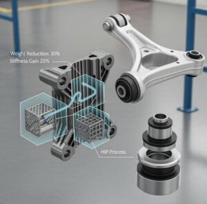
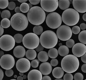
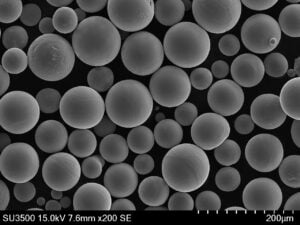
BJT製造における金属粉末モデル
BJTの製造工程では、さまざまな金属粉末モデルが使用される。これらの材料は、最終製品の効率と性能に影響を与える。
特定金属粉末モデル
- 銅(Cu)パウダー
- 説明:導電性を向上させるために使用される高導電性金属粉末。
- アプリケーション:パワー用高性能BJTに使用。
- プロパティ:優れた熱伝導性と電気伝導性
- アルミニウム(Al)パウダー
- 説明:軽量で導電性のアルミニウム粉末は、特定のBJT用途に使用される。
- アプリケーション:軽量で高熱伝導性を必要とするBJTに使用される。
- プロパティ:良好な導電性、軽量。
- ニッケル(Ni)パウダー
- 説明:耐食性と安定性で知られる。
- アプリケーション:耐久性が重要な環境で使用される。
- プロパティ:耐食性に優れ、安定した性能。
- 鉄(Fe)パウダー
- 説明:入手しやすく、磁気特性もあるため一般的に使用される。
- アプリケーション:磁気特性を必要とするBJTに使用される。
- プロパティ:マグネット式でコストパフォーマンスが高い。
- 銀(Ag)パウダー
- 説明:金属の中で最も高い導電性を持つ。
- アプリケーション:精密用途のハイエンドBJTに使用される。
- プロパティ:優れた導電性、高価。
- 金(Au)パウダー
- 説明:導電性に優れ、酸化に強い。
- アプリケーション:クリティカルで高信頼性用途のBJTに使用される。
- プロパティ:優れた導電性、高い耐食性、非常に高価。
- 亜鉛(Zn)パウダー
- 説明:良好な導電性を提供し、合金化に使用される。
- アプリケーション:汎用BJTに使用される。
- プロパティ:良好な導電性、手頃な価格。
- コバルト(Co)パウダー
- 説明:磁性と高融点で知られる。
- アプリケーション:高温安定性を必要とする特殊なBJTに使用される。
- プロパティ:磁性、高融点。
- チタン(Ti)パウダー
- 説明:軽量で強度が高く、高強度用途に使用される。
- アプリケーション:重量と強度が重要なBJTに使用される。
- プロパティ:高強度対重量比、耐腐食性。
- パラジウム(Pd)パウダー
- 説明:導電性と安定性に優れている。
- アプリケーション:高信頼性BJTに使用。
- プロパティ:良好な導電性、安定性、高価。

よくあるご質問
| 質問 | 答え |
|---|---|
| BJTとは? | バイポーラ・ジャンクション・トランジスタ(BJT)は、電気信号の増幅やスイッチングに使用される半導体デバイスである。 |
| BJTの主な種類は? | 主な種類はNPNとPNPトランジスタである。 |
| BJTにはどのような材料が使われていますか? | シリコン(Si)とゲルマニウム(Ge)が主な材料である。 |
| BJTの一般的なアプリケーションにはどのようなものがありますか? | 増幅、スイッチング、発振、調整などに使用される。 |
| NPNトランジスタとPNPトランジスタの違いは? | NPNトランジスタは電荷キャリアとして電子を使用し、PNPトランジスタはホールを使用する。 |
| BJTを使う利点は何ですか? | BJTは高い電流利得と高速スイッチングを提供する。 |
| BJTの欠点は何ですか? | 電界効果トランジスタ(FET)に比べて消費電力が大きい傾向がある。 |
| シリコンBJTの主な特性は? | 高い熱安定性と低リーク電流。 |
| BJT製造にはどのような金属粉が使われていますか? | 銅、アルミニウム、ニッケル、鉄、銀、金、亜鉛、コバルト、チタン、パラジウムの粉がよく使われる。 |
| アプリケーションに適したBJTを選ぶには? | 定格電圧、定格電流、許容損失、周波数特性などの仕様を考慮してください。 |
Additional FAQs on the BJT Process
1) How does the BJT process differ from CMOS or BiCMOS flows?
- Pure BJT processes optimize vertical current flow, thick epitaxial layers, and precise base diffusion for high gain and ft. CMOS focuses on planar MOSFETs. BiCMOS integrates high-speed BJTs with dense CMOS logic, adding extra masks for bipolar devices while sharing interconnect and isolation.
2) What sets the transition frequency (ft) and maximum oscillation frequency (fmax) in BJTs?
- ft is primarily limited by base transit time, base resistance, and junction capacitances (Cbe, Cbc). fmax depends on ft plus parasitic resistances/inductances and collector-base capacitance. Thinner bases, higher emitter efficiency, and self-aligned processes improve both.
3) Which materials and contacts are typical in modern BJT metallization?
- Standard silicon BJTs use salicided polysilicon emitters and Ni/Pt/Ti silicides. Interconnect stacks commonly use Cu with diffusion barriers (Ta/TaN) and sometimes AlCu for upper metals. For RF, Au-based pads may be used for low-resistance probing/packaging.
4) How do temperature and self-heating impact BJT performance?
- Higher junction temperature reduces β and ft, increases leakage, and risks thermal runaway in power BJTs. Layouts employ emitter ballasting, thermal vias, and heat-spreading metals; circuit-level negative feedback and SOA protection are also used.
5) What reliability tests are standard for BJT qualification?
- JEDEC/IEC-driven tests: HTOL (high-temp operating life), HTRB/HTGB, TC/TS (thermal cycling/shock), ESD (HBM/CDM), latch-up immunity (for BiCMOS), and electromigration/Time-Dependent Dielectric Breakdown on interconnects. Radiation testing (TID/SEE) is used for aerospace.
2025 Industry Trends for the BJT Process
- SiGe HBT scaling continues: Foundries push ft/fmax > 350/500 GHz via lower base resistance and raised extrinsic base structures for mmWave/6G front-ends.
- Power BJTs niche returns in analog power stages: High-voltage BJTs with enhanced safe operating area (SOA) and robust avalanche ratings complement MOSFET stages in audio, industrial drives, and automotive legacy systems.
- Advanced metal stacks: Wider adoption of copper with low-k dielectrics and cobalt caps reduces line resistance at RF; Au-free RF pads grow due to cost/compatibility.
- Integrated passives and thermal co-design: On-die MIM capacitors and thick top metals paired with compact thermal models enable higher linearity PAs and robust bias networks.
- Sustainability and traceability: RoHS/REACH compliance updates, tighter PFAS restrictions in lithography/etch consumables, and digital part passports for automotive/medical.
2025 Snapshot: BJT/SiGe HBT Performance Benchmarks (indicative)
| メートル | 2023 | 2024 | 2025 YTD | Notes/Sources |
|---|---|---|---|---|
| SiGe HBT ft (GHz) | 250–320 | 300–340 | 320–380 | Foundry PDK releases in mmWave nodes |
| SiGe HBT fmax (GHz) | 350–450 | 400–500 | 450–550 | Layout and parasitic optimization |
| Low-noise figure at 28 GHz (dB) | 1.6–2.0 | 1.4–1.8 | 1.3–1.7 | LNAs in BiCMOS RF |
| Power BJT BVceo (V) | 60–200 | 80–250 | 100–300 | Enhanced SOA and passivation |
| Au-free RF pad adoption (%) | 20–35 | 30–45 | 40–55 | Cost and assembly trends |
References: IEEE Journal of Solid-State Circuits and TED articles; foundry PDK briefs from GlobalFoundries/TSMC/Infineon; JEDEC JESD standards; IEC 60747 device data.
Latest Research Cases
Case Study 1: SiGe HBT Front-End for 6G E-Band (2025)
- Background: A telecom OEM needed lower noise and higher linearity in 71–86 GHz backhaul radios while reducing cost versus III-V solutions.
- Solution: Migrated to a 130 nm BiCMOS SiGe HBT node with ft/fmax ≈ 360/520 GHz, implemented stacked HBT PA cells, Au-free pads, and thick top-metal inductors; co-optimized thermal layout and bias.
- Results: NF 1.45 dB at 81 GHz; +18% PAE; PA Pout +1.2 dB; BOM cost −22% vs prior III-V design; improved yield by 9% using on-wafer RF DfT.
Case Study 2: Robust Power BJT with Enhanced SOA for Industrial Drives (2024)
- Background: An industrial inverter platform experienced field returns from secondary breakdown under inductive loads.
- Solution: Introduced emitter ballasting, trench isolation, and optimized edge termination; upgraded Cu/Ti barrier metallization and thicker AlCu top metal; added on-die temperature sensing for protection.
- Results: SOA margin +35% at 25 °C, +20% at 125 °C; avalanche energy rating +28%; field failure rate reduced from 340 to 70 ppm over 12 months.
専門家の意見
- Prof. Peter Ashburn, Emeritus Professor of Microelectronics, University of Southampton
- Viewpoint: “Reducing base resistance and parasitic capacitances remains the most effective path to higher ft/fmax in BJT and SiGe HBT technologies.”
- Dr. Siegfried Heinemann, Senior Fellow, Infineon Technologies
- Viewpoint: “For power BJTs, emitter ballasting and edge termination design are decisive for SOA—metallization robustness is equally critical.”
- Dr. Hua Wang, Professor of ECE, Georgia Tech
- Viewpoint: “BiCMOS with SiGe HBTs offers the best cost-performance trade for mmWave front-ends when paired with RF-centric layout and compact thermal modeling.”
Practical Tools and Resources
- Standards and reliability
- JEDEC JESD47 (stress-test-driven qualification), JESD22 (ESD/lat/temp tests), and JESD61 (SOA guidance): https://www.jedec.org
- IEC 60747 (semiconductor device specifications): https://www.iec.ch
- Foundry PDKs and design kits
- BiCMOS/SiGe HBT PDKs from GlobalFoundries, TSMC, Infineon; RF models including ft/fmax corners and thermal compact models
- Design and simulation
- Cadence SpectreRF, Keysight ADS, Ansys HFSS/Icepak, COMSOL for electro-thermal; EM/circuit co-simulation for mmWave
- Measurement references
- IEEE Microwave Magazine and T-MTT/TED tutorials on de-embedding, noise figure, and large-signal device characterization
- Reliability data and best practices
- AEC-Q101 (automotive discrete qualification) and IEC/TR guidance for power device SOA and thermal metrics
Last updated: 2025-10-16
Changelog: Added 5 targeted FAQs; introduced a 2025 KPI table for BJT/SiGe HBT performance; provided two case studies (6G E-band SiGe HBT front-end; enhanced-SOA power BJT); included expert viewpoints; linked standards, PDK, simulation, and reliability resources
Next review date & triggers: 2026-03-31 or earlier if major foundries release new SiGe HBT nodes, JEDEC/IEC standards update, or new mmWave/PA benchmarks shift state-of-the-art