
Tänk dig att bygga komplicerade strukturer atom för atom, att noggrant skapa lager av material som är så tunna att de är osynliga för blotta ögat. Detta är den värld som kemisk förångningsdeposition (CVD)är en kraftfull teknik som har revolutionerat otaliga branscher genom att möjliggöra skapandet av högpresterande, exakt konstruerade material.
Specifik introduktion till kemisk förångningsdeposition
CVD är i grund och botten en teknik för tunnfilmsdeponering där en gasformig prekursor genomgår en kemisk reaktion i en kammare, varvid en fast film avsätts på ett substrat. Tänk på det som att måla med osynlig ånga i stället för med traditionella penslar och vätskor. Denna till synes enkla process öppnar dock upp en värld av möjligheter och gör det möjligt att skapa material med specifika egenskaper som överlägsen ledningsförmåga, förbättrad slitstyrka och skräddarsydda optiska egenskaper.
De tre viktigaste stegen i CVD Process
Även om detaljerna i CVD kan variera beroende på det önskade materialet och tillämpningen, följer kärnprocessen i allmänhet tre viktiga steg:
- Leverans av prekursorer: Gasformiga prekursorer, som innehåller de element som kommer att bilda den deponerade filmen, förs in i kammaren. Dessa prekursorer kan vara enskilda element som kisel eller komplexa molekyler som innehåller olika element.
- Reaktion och deposition: Prekursorerna utsätts för olika aktiveringsmetoder, t.ex. värme, plasma eller ljus, som utlöser en kemisk reaktion. Denna reaktion bryter ner prekursorerna och gör det möjligt för de önskade elementen att kombineras och bilda den fasta filmen på substratet.
- Utrensning och avgasning: När deponeringen är klar avlägsnas alla oreagerade prekursorgaser och biprodukter från kammaren med hjälp av ett vakuumsystem.

Många fördelar med CVD-processen
CVD erbjuder flera tydliga fördelar jämfört med andra tekniker för tunnfilmsdeponering, vilket gör den till ett förstahandsval i olika tillämpningar:
- Hög konformitet: CVD möjliggör deponering av enhetliga och konforma filmer, även på komplexa tredimensionella ytor. Detta beror på att de gasformiga prekursorerna kan nå alla skrymslen och vrår på substratet, till skillnad från tekniker som PVD (Physical Vapor Deposition) som kan ha problem med invecklade geometrier.
- Exakt kontroll: Processparametrarna i CVD, t.ex. temperatur, tryck och flödeshastighet för prekursorer, kan styras exakt, vilket gör det möjligt att skräddarsy filmegenskaper som tjocklek, sammansättning och kristallinitet. Denna kontrollnivå gör det möjligt att skapa mycket skräddarsydda och konstruerade material.
- Renhet och reproducerbarhet: CVD-processer sker vanligtvis i en kontrollerad miljö, vilket minimerar kontaminering och säkerställer hög renhet hos de deponerade filmerna. Dessutom möjliggör den exakta kontrollen av processparametrarna utmärkt reproducerbarhet, vilket säkerställer konsekventa filmegenskaper i flera batcher.
- Brett materialområde: CVD kan användas för att deponera ett stort antal material, inklusive metaller, halvledare, dielektrika och till och med polymerer. Denna mångsidighet gör det till ett värdefullt verktyg för olika branscher, från mikroelektronik till solenergi.
Några nackdelar med CVD-processen
Trots sina många fördelar har CVD också vissa begränsningar:
- Hög kostnad: Att installera och underhålla ett CVD-system kan vara dyrt på grund av den specialutrustning och de exakta styrsystem som krävs.
- Långsammare deponeringshastighet: Jämfört med vissa andra deponeringstekniker kan CVD ha långsammare deponeringshastigheter, vilket kan vara en nackdel för applikationer med högvolymproduktion.
- Begränsad substratkompatibilitet: Alla material är inte lämpliga för CVD på grund av de höga temperaturer eller reaktiva miljöer som processen innebär.
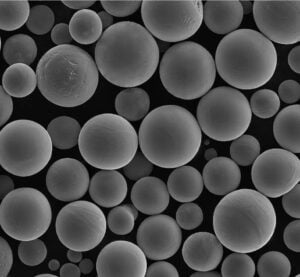
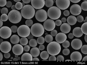
Specifika metallpulver som används i CVD
CVD kan användas för att deponera en mängd olika metallfilmer, var och en med unika egenskaper och användningsområden. Här är tio specifika metallpulvermodeller som ofta används i CVD-processer:
| Metallpulvermodell | Beskrivning och egenskaper | Tillämpningar |
|---|---|---|
| Volfram (W) | Känd för sin höga smältpunkt, utmärkta termiska stabilitet och goda elektriska ledningsförmåga. | Används i halvledarkomponenter, högtemperaturtrådar och slitstarka beläggningar. |
| Molybden (Mo) | Har hög smältpunkt, god korrosionsbeständighet och rimlig elektrisk ledningsförmåga. | Används i elektronikförpackningar, kylflänsar och eldfasta applikationer. |
| Tantal (Ta) | Hög smältpunkt, utmärkt korrosionsbeständighet och god kompatibilitet med andra material. | Används i kondensatorer, mikroelektromekaniska system (MEMS) och biomedicinska implantat. |
| Krom (Cr) | Ger bra slitstyrka, korrosionsbeständighet och hårdhet. | Används i dekorativa och skyddande beläggningar, skärverktyg och slitdelar. |
| Titan (Ti) | Biokompatibel, lätt och med god hållfasthet och korrosionsbeständighet. | Används i biomedicinska implantat, flyg- och rymdkomponenter samt sportartiklar. |
| Aluminium (Al) | Högreflekterande, lätt och god ledare av elektricitet. | Används för metallisering av integrerade kretsar, speglar och kylflänsar. |
| Koppar (Cu) | Utmärkt elektrisk ledningsförmåga och värmeledningsförmåga. | Används i elektriska ledningar, sammankopplingar i mikroelektronik och värmeväxlare. |
| Nickel (Ni) | God elektrisk ledningsförmåga, magnetiska egenskaper och korrosionsbeständighet. | Används vid elektroplätering, magnetiska inspelningsmedia och korrosionsbeständiga beläggningar. |
| Guld (Au) | Utmärkt elektrisk ledningsförmåga, korrosionsbeständighet och biokompatibilitet. | Används i elektriska kontakter, integrerade kretsar och medicintekniska produkter. |
| Platina (Pt) | Hög smältpunkt, utmärkta katalytiska egenskaper och korrosionsbeständighet. | Används i katalytiska omvandlare, bränsleceller och temperaturgivare. |


Tillämpningar av CVD: Att forma industrier
CVD:s mångsidighet sträcker sig till olika branscher och spelar en avgörande roll i många tillämpningar:
- Halvledare: CVD är avgörande för att skapa de komplicerade skikten av transistorer, kondensatorer och andra byggstenar i integrerade kretsar (IC). Den exakta kontroll och höga renhet som CVD erbjuder är avgörande för att säkerställa en tillförlitlig och effektiv drift av modern elektronik.
- Mikroelektromekaniska system (MEMS): MEMS-enheter integrerar mekaniska element med elektronik på en mikroskopisk skala. CVD möjliggör deponering av tunna filmer för olika MEMS-komponenter, t.ex. rörliga balkar, membran och elektroder.
- Solceller: CVD används för att deponera tunna filmer av material som kisel, kiselnitrid och olika transparenta ledande oxider, vilka är viktiga komponenter för att fånga upp och omvandla solljus till elektricitet.
- Optiska ytbeläggningar: Antireflexbeläggningar, speglar och filter som används i olika optiska apparater kan skapas med hjälp av CVD. Den exakta kontrollen över filmtjocklek och sammansättning gör det möjligt att skräddarsy optiska egenskaper för specifika applikationer.
- Skärande verktyg och slitstarka ytbeläggningar: CVD-beläggningar kan avsevärt förbättra slitstyrkan och hårdheten hos skärverktyg, vilket förlänger deras livslängd och förbättrar skärprestandan. Dessutom används CVD för att skapa slitstarka beläggningar för olika komponenter i maskiner och utrustning.
- Biomedicinska implantat: CVD spelar en avgörande roll i utvecklingen av biokompatibla implantat, t.ex. konstgjorda leder och stentar. Möjligheten att deponera tunna filmer med specifika egenskaper som biokompatibilitet och korrosionsbeständighet är avgörande för en lyckad implantation och långsiktig funktionalitet.
Det här är bara några exempel, och i takt med att tekniken fortsätter att utvecklas kan vi förvänta oss att CVD kommer att spela en ännu större roll när det gäller att forma olika industrier och utveckla innovativa material för framtiden.
Bortom grunderna: Avancerat CVD Tekniker
CVD-världen sträcker sig bortom den grundläggande trestegsprocessen. För att uppnå ännu större kontroll och få tillgång till ett bredare utbud av material har olika avancerade CVD-tekniker utvecklats:
- Plasmaförstärkt CVD (PECVD): Med denna teknik förs plasma in i reaktionskammaren, vilket kan öka reaktionshastigheten, förbättra filmens jämnhet och möjliggöra deponering av material som är svåra att deponera med enbart termisk CVD.
- Atomskiktsdeponering (ALD): ALD är en mycket exakt teknik där prekursorn introduceras på ett självbegränsande sätt, vilket möjliggör deponering av atomtunna filmer med exceptionell jämnhet och kontroll över tjockleken.
- Metallorganisk CVD (MOCVD): Denna teknik utnyttjar metallorganiska prekursorer, vilket ger fördelar som lägre deponeringstemperaturer och möjlighet att deponera komplexa material med specifika sammansättningar.
Genom att utforska dessa avancerade tekniker kan forskare och ingenjörer flytta fram gränserna för vad som är möjligt med CVD, vilket banar väg för utvecklingen av ännu mer sofistikerade och funktionella material.

Vanliga frågor
Här är några vanliga frågor om CVD, besvarade i tabellformat för enkel referens:
| Fråga | Svar |
|---|---|
| Vad finns det för alternativ till CVD? | Andra tekniker för tunnfilmsbeläggning är PVD (Physical Vapor Deposition), elektroplätering och spinnbeläggning. Varje teknik har sina egna fördelar och begränsningar, och det bästa valet för en specifik applikation beror på olika faktorer som önskade materialegenskaper, kostnad och produktionskrav. |
| Vilka säkerhetsåtgärder är viktiga under CVD? | CVD-processer involverar ofta farliga material och höga temperaturer. Det är viktigt att följa korrekta säkerhetsprotokoll, inklusive att bära lämplig personlig skyddsutrustning (PPE), arbeta i en väl ventilerad miljö och följa etablerade säkerhetsprocedurer för hantering av kemikalier och drift av utrustning. |
| Hur ser framtiden ut för CVD? | I takt med att forskning och utveckling fortsätter kan vi förvänta oss att framsteg inom CVD-tekniken leder till följande * Utveckling av nya prekursormaterial som möjliggör deponering av ett ännu bredare utbud av material. * Ytterligare förbättringar av processkontroll och enhetlighet, vilket möjliggör ännu mer exakt skapande av tunna filmer. * Integration av CVD med andra tillverkningsprocesser för utveckling av komplexa och multifunktionella enheter. |
Slutsats
Kemisk förångningsdeposition (CVD) är ett bevis på människans uppfinningsrikedom. Den gör det möjligt för oss att bygga upp strukturer atom för atom och skapa material med egenskaper som är skräddarsydda för specifika behov. Från de invecklade kretsar som driver våra apparater till de livräddande implantat som reparerar våra kroppar spelar CVD en avgörande roll för att forma vår värld på otaliga sätt.
I takt med att vi fördjupar oss i materialvetenskapens värld och utforskar nya tekniska gränser kommer CVD utan tvekan att fortsätta utvecklas och spela en ännu större roll i utformningen av framtiden. Med framsteg inom prekursormaterial, processkontroll och integration med andra tekniker är möjligheterna för CVD enorma och innebär en enorm potential för innovation och framsteg.
Så nästa gång du håller en smartphone i handen eller förundras över den eleganta designen hos ett modernt flygplan, kom ihåg de osynliga lagren av omsorgsfullt tillverkade material, vart och ett ett bevis på kraften i kemisk ångdeposition, ett mikroskopiskt underverk med en makropåverkan på vår värld.