
Electron beam manufacturing refers to an additive manufacturing process that uses a focused beam of high-energy electrons to selectively melt and fuse metallic powder particles together layer-by-layer to directly fabricate complex 3D components.
Also known as electron beam melting (EBM) or electron beam powder bed fusion, the process offers capabilities like build rate, material properties, surface finish and geometric freedom unmatched by traditional fabrication routes.
This guide provides an overview of electron beam manufacturing covering process capabilities, materials, applications, system suppliers, tradeoffs comparisons and FAQs when considering adoption.

Overview of Electron Beam Manufacturing Process
- Metal powder is spread uniformly over build plate
- Electron beam scans defined paths fusing powder
- Plate indexes down, new layer spread on top
- Thermal preheat maintains process temperature
- Chamber held under vacuum during build
- Supports structure where needed
- Final parts cut away and finished as needed
Electron beams offer faster, deeper penetration than lasers into conductive materials, enabling higher build rates with less residual stress.
Materials Used in Electron Beam Manufacturing
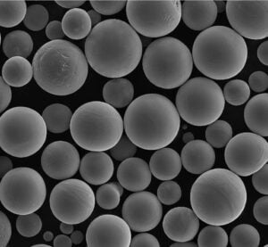
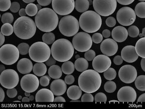
A wide range of alloys are processed, each optimized for chemistry and particle size distribution:
| Material | Common Alloys | Overview |
|---|---|---|
| Titanium alloy | Ti6Al4V, Ti6Al4V ELI | Aerospace grade blends with high strength, low weight |
| Nickel alloy | Inconel 718, 625, Haynes 282 | Heat/corrosion resistant superalloys for turbines |
| Cobalt chrome | CoCrMo | Biocompatible, wear resistant alloy for implants |
| Stainless steel | 17-4PH, 316L, 304L | High strength with corrosion resistance |
| Tool steel | H13, Maraging Steel | Extreme hardness/wear resistance |
| Aluminum alloy | Scalmalloy | Custom al width rapid solidification rates |
Advantages like grain and defect structure control promote enhanced mechanical properties.
Characteristics and Tolerances
In addition to tailored alloy properties, key process capabilities include:
| Attribute | Description |
|---|---|
| Surface finish | As low as 5 μm roughness, smooth enough for final use depending on geometry, no finishing required |
| Feature resolution | Fine details down to ~100 μm supported by process parameters |
| Accuracy | ± 0.2% with 50 μm deviation over 100 mm part dimensions |
| Density | Over 99.8% of theoretical max, highest of metal AM methods |
| Build size | Components over 1000 mm length feasible, dependent on system model |
| Prototyping | Capable of single to small batch production, ideal for engineering models requiring metals |
| Production | Aerospace and medical industries beginning to certify process for end-use parts production |
The consistency and quality allow high demand applications.
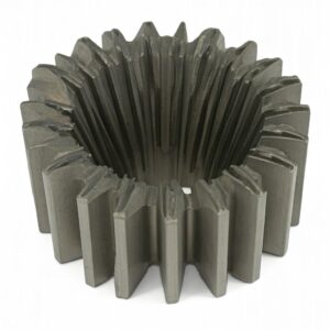
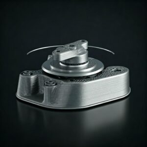
Electron Beam Manufacturing Applications
| Industry | Uses | Component Examples |
|---|---|---|
| Aerospace | Structural components, engine parts | Turbine blades, frames, mounts |
| Medical | Orthopedic implants, surgical tools | Hip, knee, skull implants, clamps |
| Automotive | Lightweight performance components | Turbine wheels, manifolds |
| Industrial | End-use metal production | Lightweight robot arms, fluid handling parts |
Additional specialty uses leverage design, material, performance synergies.


System Manufacturers and Pricing
| Manufacturer | Description | Base Price Range |
|---|---|---|
| Arcam (GE) | Pioneers with a range of EBM system models | $1.5M – $2M |
| Velo3D | Advanced systems promise finer details and taller builds | $$$$ |
| Jeol | Research and small-scale production focused | $$$ |
Operational expenses around materials, argon, electricity can range from $100-$1000+ per day depending on builds.
Tradeoffs of Electron Beam vs Other Processes
Pros:
- Higher build rate than powder bed laser fusion
- Lower residual stress than laser methods
- Exceptional accuracy and surface finish
- High purity input material for properties
- High potential future production volumes
Cons:
- Still maturing relative to other powder bed technologies
- Size capability not as large laser methods
- Material availability still widening
- Higher equipment cost of ownership
- Constraints around geometries requiring support
For the right applications, unparalleled performance potential.
FAQs
What determines maximum part size?
System model’s maximum scan area, scan strategy limitations, thermal stresses, powder spreadability constraints, and number of components define size capabilities up to ~800mm lengths tested.
How does the process affect material properties?
Rapid cooling rates from controlled thermal profiles impart fine microstructures enhancing strength. Parameters are balanced against residual stresses.
What determines surface finish capability?
Spot size, beam power, scan strategy, subsequent powder layer thickness, particulate contamination, and thermal gradient influences combine to enable exceptional as-fabricated surface quality.
What safety precautions are required?
In addition to powder handling protections, electron beam systems require certified rooms with Faraday cage shielding, safety interlocks, maximum occupancy exposure time calculation.
What are typical post-processing steps?
Post processes like hot isostatic pressing to reduce porosity, heat treatments for enhanced mechanical performance, and subtractive machining are commonly employed to finish components.